0 · Recall Warm-up
Answer from memory first. Answers are in the Answer Vault at the bottom.
- Booth: what does the pair (Q₀, Q₋₁) = 01 trigger? from Lesson 2.1.3
- A ripple adder's last carry is ready after? from Lesson 2.1.2
- What does
POP R1do with a downward stack? from Lesson 1.3.2
1 · The Hook
🎣
"Fetch the instruction at PC" is one line in Phase 1. Inside the CPU it is three moves between specific registers: the address goes to the register wired to the address bus, the data comes back into the register wired to the data bus, then moves to the register the decoder reads. This lesson names those registers and a notation, register transfer language, for writing the moves.
2 · Predict First
🤔
Memory is connected to the CPU through exactly two registers: one that drives the address bus and one that connects to the data bus. Write the instruction fetch as three register-to-register moves.
Make a guess in your head. The answer opens Section 3.
3 · Core Concept
💡
Predict First — the answer
MAR ← PC; MDR ← M[MAR] (and PC ← PC + 4); IR ← MDR.
The CPU's registers
| Register | Holds | Width |
|---|---|---|
| PC (program counter) | address of the next instruction | address bits |
| IR (instruction register) | the instruction being executed (the decoder reads it) | instruction length |
| MAR (memory address register) | the address for the current memory access; drives the address bus | address bits |
| MDR (memory data register, also MBR) | data just read from memory, or data about to be written | data bus width |
| R0 … Rn−1 (general-purpose registers) | operands and results | word size |
| SP | top of the stack (Lesson 1.3.2) | address bits |
| PSW / flags | Z, N, C, V and control bits | a few bits |
| Temporary registers | internal values the programmer cannot see (Y, Z in Lesson 2.2.2) | word size |
Registers the programmer's instructions can name (GPRs, SP, PC through jumps, flags through branches) are visible; MAR, MDR, IR and temporaries are invisible to programs.
Register transfer notation (RTL)
R1 ← R2: copy R2 into R1 (R2 unchanged).R1 ← R2 + R3: through the ALU.MDR ← M[MAR]: memory read;M[MAR] ← MDR: memory write.IR(address): the address field of IR.if (Z = 1) then PC ← PC + offset: conditional transfer.- Transfers in the same clock step are separated by commas:
MAR ← PC, PC ← PC + 4.
Fetch and two executes in RTL (32-bit words, byte addresses)
Fetch:     T1: MAR ← PC
           T2: MDR ← M[MAR], PC ← PC + 4
           T3: IR ← MDR
LOAD R1, X (direct):
           T4: MAR ← IR(address)
           T5: MDR ← M[MAR]
           T6: R1 ← MDR
ADD R1, R2, R3:
           T4: R1 ← R2 + R3
How many steps each transfer takes depends on the wiring between registers. That is the datapath, the topic of the next two lessons.
Memory timing words
A memory read is started by placing the address in MAR and raising Read; the data reaches MDR when memory signals MFC (memory function complete). A step that must wait for it is marked WMFC (wait for MFC). Unless a question says otherwise, assume memory completes within one step.
4 · Visual
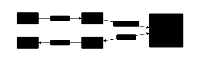
Fetch: PC → MAR → memory → MDR → IR.
5 · Worked Examples
Example 1 Easy
A CPU has 32-bit addresses and a 64-bit data bus. How wide are MAR and MDR?
Solution
MAR = 32 bits (address); MDR = 64 bits (data bus width).
Example 2 Medium
Write STORE R2, X (direct) in RTL after the fetch.
Solution
MAR ← IR(address), MDR ← R2, then M[MAR] ← MDR. (The first two can share a step if the datapath allows it.)
Example 3 GATE
Which registers change during the fetch of a 4-byte instruction?
Solution
MAR (gets PC), MDR (gets the instruction), PC (+4) and IR (gets the instruction).
6 · GATE Traps
⚠️
- MAR holds an address, MDR holds data: don't swap them.
- IR holds the current instruction itself; PC holds the next instruction's address.
- MAR, MDR, IR are invisible to the programmer.
- Commas in RTL mean "same step", which needs separate hardware paths.
7 · Memory Hook
🧠
"MAR = Memory's Address, MDR = Memory's Data." Every memory access goes through this pair.
8 · Connect the Dots
You can name every register and write any instruction as register transfers. Next: the cheapest wiring, a single internal bus, which forces those transfers into a strict one-at-a-time order of control steps.
9 · Self-Test
GATE format. Try every question before opening the vault.
Q1MCQ1 markMAR
Which register drives the address bus?
- (A) IR
- (B) MDR
- (C) MAR
- (D) PC
Q2NAT1 markMDR width
A processor has a 48-bit address bus and a 128-bit data bus. How many bits wide is MDR?
Numerical answer: ________
Q3MSQ2 marksVisible registers
Which registers are normally invisible to machine-language programs?
- (A) IR
- (B) MDR
- (C) R5 (general-purpose)
- (D) MAR
Q4MCQ1 markRTL
MAR ← PC, PC ← PC + 4 means:
- (A) MAR gets PC + 4
- (B) both transfers happen in the same clock step
- (C) PC is copied to MAR, then later PC is incremented
- (D) the PC is incremented before MAR is loaded
Q5NAT1 markSteps
Using the lesson's RTL, how many steps do fetch plus execute take for LOAD R1, X?
Numerical answer: ________
10 · Rule Card
- PC: next instruction address. IR: current instruction. MAR: address bus. MDR: data bus.
- Memory read: MAR ← addr; MDR ← M[MAR] (Read, wait MFC). Write: MAR, MDR set; M[MAR] ← MDR.
- RTL: ← transfer; commas = same step; IR(address) = address field.
- Fetch: MAR ← PC; MDR ← M[MAR], PC ← PC + 4; IR ← MDR.
11 · Concept Ledger
Unlocked in this lesson. From here on, these terms may be used.
PC, IR, MAR, MDRgeneral-purpose registersvisible vs invisible registerstemporary registersregister transfer notation (RTL)same-step transfersRead and MFC/WMFC
12 · Answer Vault
Answer Vault
Try the questions first. Open when you are ready to check.
Recall Warm-up
- A ← A + M (end of a run of 1s).
- n × t_c.
- R1 ← M[SP]; SP ← SP + w.
Self-Test
Q1 Answer: (C)1 mark
All addresses go out through MAR.
- (A) is wrong: IR holds the instruction.
- (B) is wrong: MDR connects to the data bus.
- (D) is wrong: The PC's value is copied into MAR first.
Re-read: Lesson 2.2.1 — CPU registers and register transfer notation: PC, IR, MAR, MDR, GPRs, flags, SP
Q2 Answer: 1281 mark
MDR matches the data bus.
Re-read: Lesson 2.2.1 — CPU registers and register transfer notation: PC, IR, MAR, MDR, GPRs, flags, SP
Q3 Answer: (A) (B) (D)2 marks
Programs name general-purpose registers; MAR, MDR and IR are internal.
- (C) is wrong: GPRs are visible.
Re-read: Lesson 2.2.1 — CPU registers and register transfer notation: PC, IR, MAR, MDR, GPRs, flags, SP
Q4 Answer: (B)1 mark
Comma = same step. MAR gets the old PC.
- (A) is wrong: MAR gets the value PC had at the start of the step.
- (C) is wrong: They happen together.
- (D) is wrong: Both use values from the start of the step.
Re-read: Lesson 2.2.1 — CPU registers and register transfer notation: PC, IR, MAR, MDR, GPRs, flags, SP
Q5 Answer: 61 mark
T1–T3 fetch, T4–T6 execute.
Re-read: Lesson 2.2.1 — CPU registers and register transfer notation: PC, IR, MAR, MDR, GPRs, flags, SP