0 · Recall Warm-up
Answer from memory first. Answers are in the Answer Vault at the bottom.
- Minimal SOP of the majority function (1 when at least two of A, B, C are 1)? from Lesson 4.1.1
- What does a NAND–NAND circuit realise? from Lesson 3.2.2
- How many rows in the truth table of 4 variables? from Lesson 3.1.1
1 · The Hook
🎣
A light at a pedestrian crossing should turn on when at least two of three sensors see someone. Turning that sentence into a working circuit is exactly the design method of this lesson: words → truth table → K-map → gates. And because every gate takes a few nanoseconds to react, we also learn to find the slowest path through a circuit, which limits how fast it can work.
2 · Predict First
🤔
A signal passes through a NOT gate (1 ns), then an AND gate (2 ns), then an OR gate (2 ns). How long after the input changes can the output be trusted?
Make a guess in your head. The answer opens Section 3.
3 · Core Concept
💡
Predict First — the answer
1 + 2 + 2 = 5 ns (delays along a path add up).
🗣️
In plain words
A combinational circuit has no memory: its outputs depend only on the inputs right now. To analyse one, write each gate's output from the inputs forward. To design one, write the truth table, minimise it with a K-map and draw the gates. Each gate has a propagation delay; the circuit's delay is the total along its slowest input-to-output path.
1. Combinational vs sequential
- Combinational: output = function of current inputs only (adders, multiplexers, decoders). Phase 5.
- Sequential: output also depends on stored past values (flip-flops, counters). Phase 6.
2. Analysis
Label every gate output with its expression, from inputs to outputs, then simplify or build the truth table (Lesson 3.1.1 §4).
3. Design procedure
- Name the inputs and outputs.
- Write the truth table from the specification.
- Minimise each output (K-map, Phase 4).
- Draw the circuit (AND–OR, or NAND–NAND).
Example: majority of three (output 1 when at least two inputs are 1): minterms 3, 5, 6, 7 → F = AB + BC + CA.
4. Propagation delay and the critical path
- Each gate output changes some time after its inputs change: its propagation delay.
- The delay of the whole circuit is the largest sum of delays over all input-to-output paths: the critical path.
- A two-level SOP circuit has 2 gate delays (plus 1 if inverted inputs need NOT gates).
5. Hazards (glitches)
F = AB + A'C with B = C = 1: when A goes from 1 to 0, AB turns off at once but A'C turns on only after the inverter delay, so F can dip to 0 for a moment: a static-1 hazard. Adding the consensus term BC (redundant logically) keeps F = 1 during the change. In K-map terms: two adjacent 1s covered by different groups can glitch; a group covering both removes the hazard.
4 · Visual
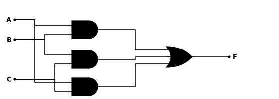
The majority circuit F = AB + BC + CA: three ANDs and a 3-input OR (two gate delays).
5 · Worked Examples
Example 1 Easy
Is a circuit whose output depends on the previous input combinational?
Solution
No: it needs memory, so it is sequential.
Example 2 Medium
Gate delays: NOT 1 ns, AND 2 ns, OR 3 ns. What is the delay of F = AB' + C'D built as NOT → AND → OR?
Solution
Critical path through a NOT: 1 + 2 + 3 = 6 ns.
Example 3 GATE
Which redundant term removes the static-1 hazard in F = AB + A'C?
Solution
The consensus term BC.
6 · GATE Traps
⚠️
- Delay is the maximum path sum, not the sum of all gate delays in the circuit.
- Count inverters on the path if inputs must be complemented.
- A redundant consensus term doesn't change the function but can remove a glitch.
- Combinational circuits have no feedback loops and no memory.
7 · Memory Hook
🧠
"Words → truth table → K-map → gates. Delay = slowest path."
8 · Connect the Dots
The most important combinational circuit in a computer adds numbers. The next lesson builds the half adder, the full adder and the ripple-carry adder, and times how long the carry takes to ripple through.
9 · Self-Test
GATE format. Try every question before opening the vault.
Q1MCQ1 markDefinition
A circuit is combinational if:
- (A) it has feedback from outputs to inputs
- (B) it uses a clock
- (C) it contains flip-flops
- (D) its outputs depend only on the present inputs
Q2NAT1 markDelay
A path goes through an XOR (3 ns), an AND (2 ns) and an OR (2 ns). Delay along this path, in ns?
Numerical answer: ________
Q3NAT2 marksCritical path
F = (A ⊕ B)C + D. Delays: XOR 4 ns, AND 2 ns, OR 2 ns. What is the delay from the inputs to F?
Numerical answer: ________
Q4MCQ1 markDesign
Which expression is the majority function of A, B, C?
- (A) A ⊕ B ⊕ C
- (B) A + B + C
- (C) AB + BC + CA
- (D) ABC
Q5MCQ1 markHazard
To remove the static-1 hazard in F = AB + A'C, add:
- (A) AC
- (B) BC
- (C) A'B
- (D) ABC
10 · Rule Card
- Combinational: outputs depend only on current inputs; sequential circuits remember.
- Design: specification → truth table → K-map → gates (AND–OR or NAND–NAND).
- Circuit delay = largest sum of gate delays along any input-to-output path (critical path).
- Static-1 hazard between adjacent 1s in different groups; fix with the consensus term.
11 · Concept Ledger
Unlocked in this lesson. From here on, these terms may be used.
combinational circuitsequential circuit (preview)circuit analysisdesign proceduremajority functionpropagation delaycritical pathgate levelsstatic hazardglitchhazard removal with consensus terms
12 · Answer Vault
Answer Vault
Try the questions first. Open when you are ready to check.
Recall Warm-up
- AB + BC + CA.
- A sum of products.
-
Self-Test
Q1 Answer: (D)1 mark
No memory.
- (A) is wrong: Feedback creates memory.
- (B) is wrong: Clocks are for sequential circuits.
- (C) is wrong: That makes it sequential.
Re-read: Lesson 5.1.1 — Combinational circuits: analysis, design and propagation delay
Q2 Answer: 71 mark
3 + 2 + 2.
Re-read: Lesson 5.1.1 — Combinational circuits: analysis, design and propagation delay
Q3 Answer: 82 marks
Through the XOR, AND and OR: 4 + 2 + 2.
Re-read: Lesson 5.1.1 — Combinational circuits: analysis, design and propagation delay
Q4 Answer: (C)1 mark
1 when at least two inputs are 1.
- (A) is wrong: Parity.
- (B) is wrong: At least one.
- (D) is wrong: All three.
Re-read: Lesson 5.1.1 — Combinational circuits: analysis, design and propagation delay
Q5 Answer: (B)1 mark
The consensus term of AB and A'C.
- (A) is wrong: Changes the function.
- (C) is wrong: Changes the function.
- (D) is wrong: Too small to cover the transition.
Re-read: Lesson 5.1.1 — Combinational circuits: analysis, design and propagation delay